Test & Burn-In Sockets
Gold Technologies, Inc. (Goldtec) design and manufacture Test & Burn-in sockets


HIGH PERFORMANCE TEST SOCKETS
Applications
Engineering test & Validation
Product Characterization including RF
System Level Test in PCB
Volume Manufacturing with Test Handler
Board to Board Interconnect
Product Verification
Chipset Testing & Recovery
Failure Analysis
Standard or Custom IC Package
CSP, BGA, LGA, QFP, QFN/MLF, PGA, SOIC, SOJ, TSOP, TO, DIP, SIP, SOT
-55°C to +155°C Testing
0.4mm to 1.27mm Device Pitch
Standard or custom matched existing PCB Footprint
1 to 4 weeks lead time
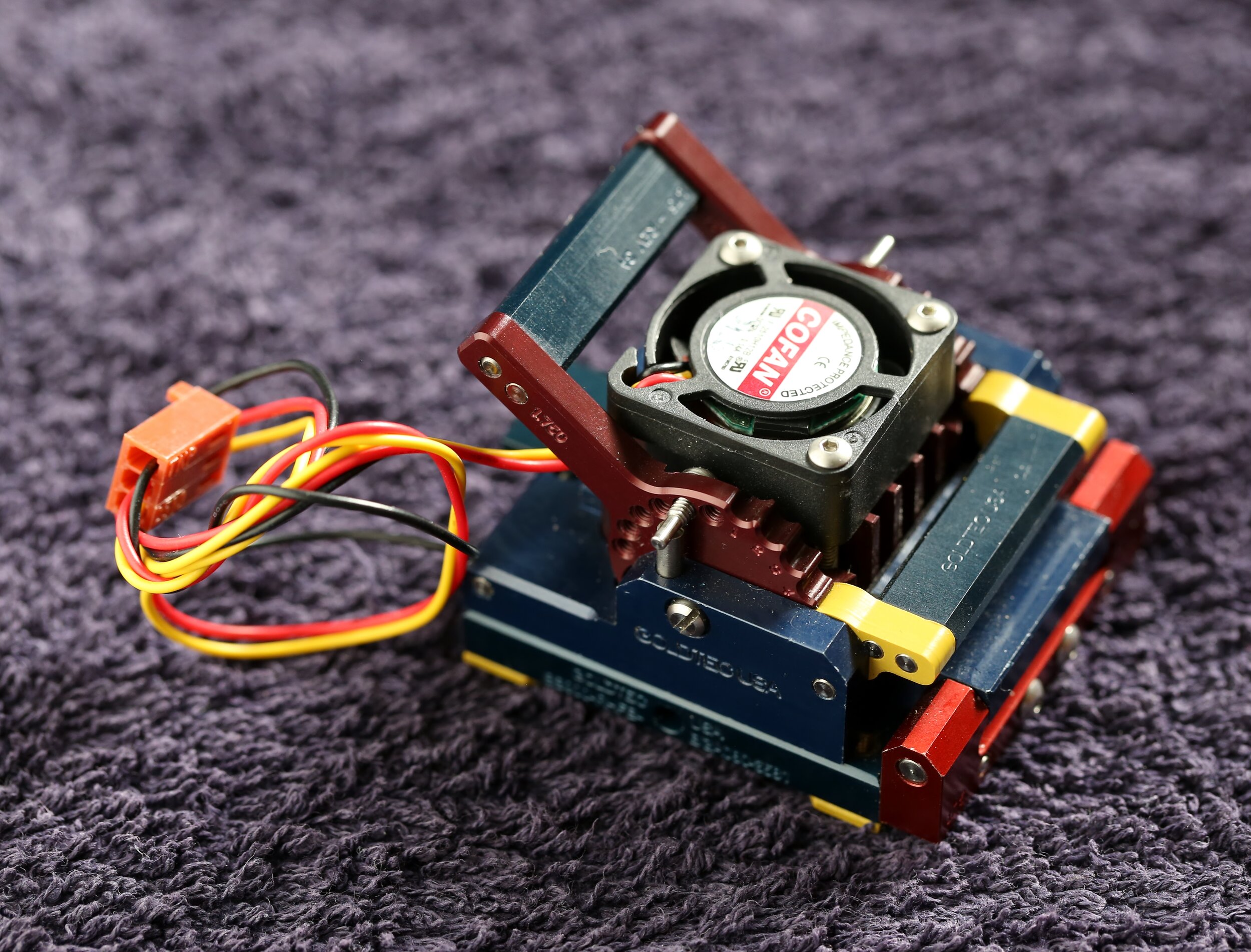
High Wattage or Heat Load – >80W dissipation
Custom thermocouple fixture with heat sink, fan and RTD element

BURN-IN Test Sockets
Applications
Burn-In
BIST & DFT
-55 °C to +155°C Testing
0.4mm to 1.27mm Device Pitch
Standard PCB Footprint
Standard or Custom IC Package
CSP, BGA, LGA, QFP, QFN/MLF, PGA, SOIC, SOJ, TSOP, TO, DIP, SIP, SOT
4 to 6 weeks lead time
Economical Socket for High volume testing
Minimum to no tooling fee

Strip ContactorS
Metal frame that functions as a stiffener and mount to PCB
Universal footprint
Replaceable cartridge